| CPC H04L 7/0079 (2013.01) [H03M 1/1245 (2013.01); H04W 56/005 (2013.01)] | 24 Claims |
|
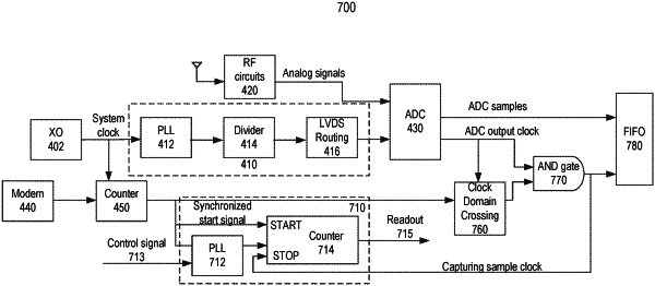
1. A method for determining an analog-to-digital converter (ADC) output timing in a user equipment, comprising:
obtaining a set of ADC samples generated by an ADC based on analog signals and an ADC input clock;
generating, at a first time point, a start signal indicating a starting point of capturing the set of ADC samples;
synchronizing, at a second time point, the start signal and a system clock;
generating, at a third time point, a capturing sample clock for capturing the set of ADC samples;
inputting the synchronized start signal and the capturing sample clock to a counter to determine a time difference between the second time point and the third time point; and
determining an ADC output timing of the set of ADC samples based on the time difference.
|