| CPC H03M 1/0604 (2013.01) [H03M 1/0626 (2013.01); H03M 1/0687 (2013.01); H03M 1/502 (2013.01)] | 20 Claims |
|
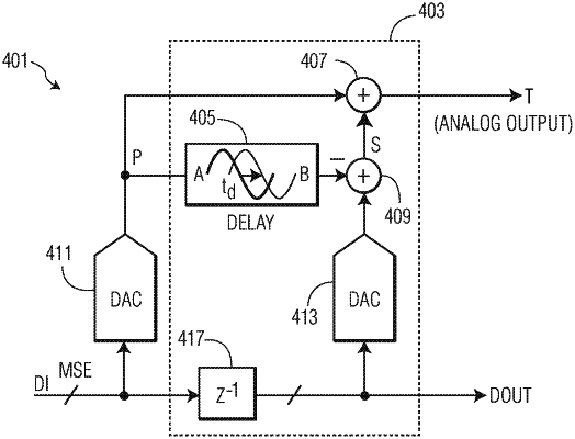
1. A circuit comprising:
a digital circuit including a digital output for producing a series of digital signal values;
a first data path from the digital output, the first data path including an analog delay circuit, the first data path for producing a first analog delay signal from the digital output the digital circuit;
a second data path from the digital output, the second data path including a digital delay circuit and a digital to analog converter for producing a second analog delay signal from the digital output of the digital circuit;
an analog circuit output for producing an analog output signal having values over time corresponding to the digital signal values of the series, wherein the first analog delay signal and the second analog delay signal are used to adjust a later analog output signal value of the analog output signal that is produced by the analog circuit output subsequent to a former analog output signal value of the analog output signal produced by the analog circuit output that corresponds to a digital signal value of the series with a metastable error.
|