| CPC H03L 7/0891 (2013.01) | 5 Claims |
|
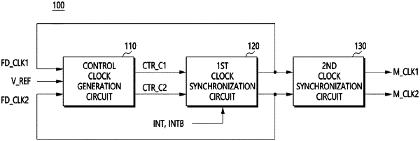
1. A clock generation circuit comprising:
a control clock generation circuit comparing a voltage level of a reference voltage with each voltage level of a first feedback clock signal and a second feedback clock signal to generate a first control clock signal and a second control clock signal;
a first clock synchronization circuit making the first feedback clock signal and the second feedback clock signal transit in synchronization with the first control clock signal and the second control clock signal, wherein the first clock synchronization circuit is configured to generate each of the first feedback clock signal and the second feedback clock signal based on both of the first control clock signal and the second control clock signal; and
a second clock synchronization circuit generating a first phase clock signal and a second phase clock signal in synchronization with a time point when each of the first feedback clock signal and the second feedback clock signal transitions.
|