| CPC H03K 5/01 (2013.01) [H03K 19/20 (2013.01); H03K 2005/00013 (2013.01)] | 20 Claims |
|
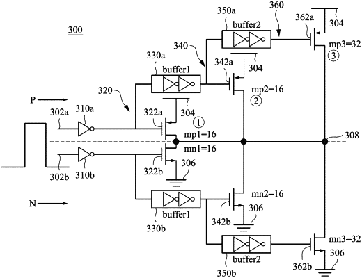
1. A driving buffer, comprising:
an input configured to receive an input signal with a rising edge or falling edge of digital data;
an output; and
a plurality of delay paths, each connected between the input and the output and being configured to delay the input signal by a respective amount of time and including a driver having a respective gain, at least two of the delay paths being configured to delay the input signal by different amounts of time from each other
wherein at least two of drivers connected to respective delay cells each comprise a transistor, the transistors in the at least two drivers having different sizes from each other.
|