| CPC H03F 3/213 (2013.01) [H01L 21/4853 (2013.01); H01L 23/49503 (2013.01); H01L 23/4952 (2013.01); H01L 23/49562 (2013.01); H01L 23/49575 (2013.01); H01L 23/49861 (2013.01); H01L 23/66 (2013.01); H01L 24/48 (2013.01); H03F 1/56 (2013.01); H05K 1/181 (2013.01); H01L 2223/665 (2013.01); H01L 2223/6655 (2013.01); H01L 2224/48139 (2013.01); H03F 2200/451 (2013.01)] | 23 Claims |
|
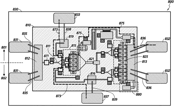
1. A packaged semiconductor chip comprising:
a semiconductor substrate;
a radio-frequency (RF) input contact pad implemented on the semiconductor substrate;
an RF output contact pad implemented on the semiconductor substrate;
first and second direct-current (DC) contact pads implemented on the semiconductor substrate;
a first amplifier stage implemented on the semiconductor substrate, the first amplifier stage comprising one or more first transistors and having an input coupled with the RF input contact pad;
a second amplifier stage implemented on the semiconductor substrate, the second amplifier stage comprising one or more second transistors and having an input coupled with an output of the first amplifier stage and an output coupled with the RF output contact pad;
an input bias coupling path implemented on the semiconductor substrate and electrically routing the first DC contact pad to the second DC contact pad and the input of the first amplifier stage;
an output bias coupling path implemented on the semiconductor substrate and electrically routing an output bias signal to the output of the second amplifier stage and to the output of the first amplifier stage; and
a lead frame comprising:
one or more RF input pins electrically coupled to the RF input contact pad;
one or more RF output pins electrically coupled to the RF output contact pad; and
first and second input bias pins electrically coupled to the first and second DC contact pads, respectively.
|