| CPC H01L 31/02002 (2013.01) [H01L 31/0203 (2013.01)] | 14 Claims |
|
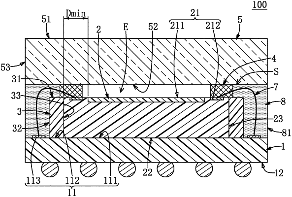
1. A sensor package structure, comprising:
a plurality of metal wires;
a substrate having a first board surface and a second board surface that is opposite to the first board surface;
a sensor chip disposed on the first board surface and electrically coupled to the substrate through the metal wires, wherein a top surface of the sensor chip includes a sensing region, and the sensing region is spaced apart from an outer lateral side of the sensor chip by a distance less than 300 μm;
a ring-shaped solder mask frame disposed on the first board surface of the substrate and arranged at an inner side of the metal wires, wherein the ring-shaped solder mask frame surrounds and contacts the outer lateral side of the sensor chip;
a ring-shaped support, wherein a part of each of the metal wires is embedded in the ring-shaped support that is disposed on a top side of the ring-shaped solder mask frame and the top surface of the sensor chip; and
a light permeable member having a first surface and a second surface that is opposite to the first surface and that is disposed on the ring-shaped support, wherein the second surface of the light permeable member, the ring-shaped support, and the sensor chip jointly define an enclosed space.
|