| CPC H01L 29/872 (2013.01) [H01L 29/1608 (2013.01); H01L 29/456 (2013.01); H01L 29/66143 (2013.01)] | 19 Claims |
|
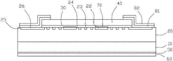
1. A silicon carbide power diode device, comprising:
a silicon carbide substrate;
a silicon carbide epitaxial layer on a first surface of the silicon carbide substrate, the carbide epitaxial layer having an active region, and the active region having a surface away from the silicon carbide substrate;
a Schottky metal layer on the surface of the active region, the active region having an N-type region and a plurality of P-type regions, the N-type region extending from the surface of the active region toward the silicon carbide substrate, the P-type regions are spaced apart from each other in the N-type region, and extend to the surface of the active region; and
a plurality of ohmic contact layers on a surface of some of the P-type regions and set between the P-type regions and the Schottky metal layer;
wherein the plurality of P-type regions include a plurality of first P-type regions and a plurality of second P-type regions, wherein between neighboring ones of the first P-type regions there is at least one of the second P-type region, the ohmic contact layers being on the surface of the first P-type regions.
|