| CPC H01L 29/87 (2013.01) [H01L 29/0684 (2013.01)] | 17 Claims |
|
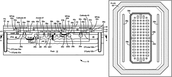
1. A diode comprising:
a substrate having a first type dopant;
a buried layer having a second type dopant and formed within the substrate;
an epitaxial layer having the second type dopant and formed above the buried layer;
a plurality of regions having the first type dopant within the epitaxial layer, wherein the plurality of regions comprises a first region, a second region, a third region, and a fourth region;
a base well having the first type dopant and located within the epitaxial layer and in contact with the third and fourth regions;
a first well having the second type dopant and formed in the epitaxial layer;
a second well having the first type dopant, and formed in the epitaxial layer, the second well extending into the first region;
a third well having the first type dopant located in the epitaxial layer and connected to the base well and connected to the second region and to the fourth region;
an anode;
a first heavily doped region having the second type dopant connected to the anode and the base well;
a second heavily doped region having the second type dopant connected to the anode and the base well; and
a cathode,
wherein in a reverse-bias mode, the diode is an electrostatic discharge (ESD) clamp and forms parasitic transistors comprising a first bipolar junction transistor (BJT), a second BJT and a third BJT.
|