| CPC H01L 29/78609 (2013.01) [G02F 1/136222 (2021.01); G02F 1/1368 (2013.01); H01L 29/41733 (2013.01); H01L 29/78696 (2013.01)] | 9 Claims |
|
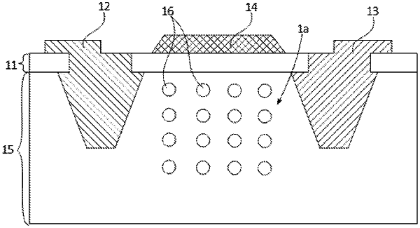
1. A thin film transistor structure, comprising:
a base;
a source electrode;
a drain electrode configured to connect to a pixel electrode;
a grid electrode;
an insulating layer;
a slow-release electrode;
wherein the source electrode, the drain electrode and the grid electrode are provided on the base, and a channel is formed between the source electrode and the drain electrode;
the insulating layer is provided on a side of the source electrode and the drain electrode, and filled in the channel;
the slow-release electrode is provided in the insulating layer, and at least a part of the slow-release electrode is provided inside the channel; and
when the grid electrode is energized, the slow-release electrode is charged; and when the grid electrode is powered off after energized, a voltage difference between the slow-release electrode and the drain electrode is smaller than a voltage difference between the slow-release electrode and the source electrode,
the thin film transistor structure further comprises a plurality of slow-release electrodes;
wherein at least part of each slow-release electrode is provided inside the channel; and
each slow-release electrode comprises at least one spherical or hollow hemispherical structure.
|