| CPC H01L 29/7823 (2013.01) [H01L 29/0865 (2013.01); H01L 29/0882 (2013.01); H01L 29/1095 (2013.01); H01L 29/402 (2013.01); H01L 29/42356 (2013.01); H01L 29/42368 (2013.01); H01L 29/42376 (2013.01); H01L 29/512 (2013.01); H01L 29/66659 (2013.01); H01L 29/66681 (2013.01); H01L 29/7835 (2013.01); H01L 27/0733 (2013.01); H01L 29/0847 (2013.01)] | 20 Claims |
|
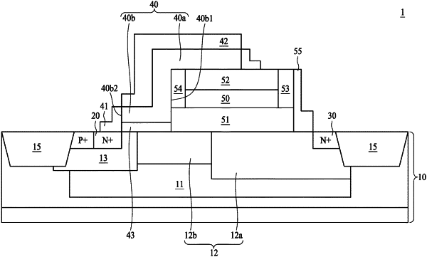
16. A semiconductor device, comprising:
a substrate having a top surface, comprising:
a first drift region with a first conductivity type, extending from the top surface of the substrate into the substrate;
a second drift region with the first conductivity type, extending from the top surface of the substrate into the substrate and adjacent to the first drift region; and
a drain region of the first conductive type within the first drift region;
a field plate over the substrate; and
a gate electrode having a first portion and a second portion, wherein the first portion of the gate electrode is located over the field plate;
a first dielectric layer in contact with the top surface of the substrate and under the field plate; and
a first spacer in contact with the top surface of the substrate and a side of the first dielectric layer;
wherein a side of the first spacer is aligned with a boundary of the drain region and the first drift region.
|