| CPC H01L 29/7787 (2013.01) [H01L 21/0254 (2013.01); H01L 21/02576 (2013.01); H01L 21/02579 (2013.01); H01L 23/291 (2013.01); H01L 23/3171 (2013.01); H01L 29/2003 (2013.01); H01L 29/205 (2013.01); H01L 29/207 (2013.01); H01L 29/66462 (2013.01)] | 14 Claims |
|
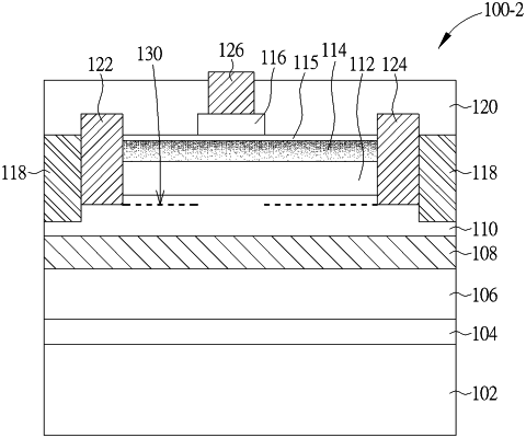
1. A semiconductor structure, comprising:
a buffer layer, disposed on a substrate;
a channel layer, disposed on the buffer layer;
a barrier layer, disposed on the channel layer;
a doped compound semiconductor layer, disposed on the barrier layer; and
a composition gradient layer, disposed between the barrier layer and the doped compound semiconductor layer, wherein the barrier layer and the composition gradient layer include a same group III element and a same group V element, and an atomic percentage of the same group III element in the composition gradient layer is gradually increased in a direction from the barrier layer to the doped compound semiconductor layer.
|