| CPC H01L 29/7436 (2013.01) [H01L 27/0259 (2013.01); H01L 29/0692 (2013.01); H02H 9/046 (2013.01); H01L 27/0285 (2013.01); H01L 27/0292 (2013.01); H01L 29/7408 (2013.01)] | 20 Claims |
|
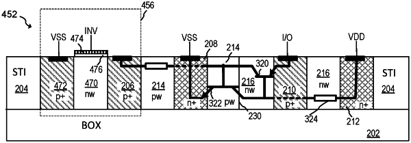
1. A semiconductor device comprising:
an n-doped region disposed over an insulating layer;
a p-doped region disposed over the insulating layer adjacent to the n-doped region, wherein an interface between the n-doped region and the p-doped region form a first diode junction;
a plurality of segmented p-type anode regions disposed over the insulating layer, each of the plurality of segmented p-type anode regions being surrounded by the n-doped region, wherein a doping concentration of the plurality of segmented p-type anode regions is greater than a doping concentration of the p-doped region; and
a plurality of segmented n-type cathode regions disposed over the insulating layer, each of the plurality of segmented n-type cathode regions being surrounded by the p-doped region, wherein a doping concentration of the plurality of segmented n-type cathode regions is greater than a doping concentration of the n-doped region.
|