| CPC H01L 29/66348 (2013.01) [H01L 29/0696 (2013.01); H01L 29/7397 (2013.01)] | 10 Claims |
|
1. A power semiconductor device, comprising an emitter, a collector and a gate electrode, a first semiconductor layer of a first conductivity type being provided on the collector, a second semiconductor layer of a second conductivity type being provided on the first semiconductor layer of the first conductivity type, and a lightly-doped third semiconductor drift region of the second conductivity type being provided on the second semiconductor layer of the second conductivity type;
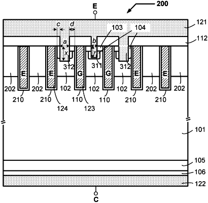
the lightly-doped third semiconductor drift region of the second conductivity type being provided therein with one or more gate trenches extending from an upper surface of the lightly-doped third semiconductor drift region of the second conductivity type into the third semiconductor drift region, one or more dummy gate trenches parallel to the gate trenches and located near the gate trenches, an electrically floating seventh semiconductor region of the first conductivity type located between adjacent dummy gate trenches and a fourth semiconductor region of the first conductivity type located at a side of the gate trench; a gate electrode being provided in the gate trench, a dummy gate electrode being provided in the dummy gate trench, and the dummy gate electrode being coupled to the emitter electrode;
a heavily-doped fifth semiconductor region of the second conductivity type and a heavily-doped sixth semiconductor region of a first conductivity type being provided on the fourth semiconductor region of a first conductivity type, the heavily-doped fifth semiconductor region of the second conductivity type adjoining the same side wall of the gate trench, and the heavily-doped sixth semiconductor region of a first conductivity type adjoining the fifth semi conductor region;
an insulating dielectric layer located on the lightly-doped third semiconductor drift region of the second conductivity type;
wherein a first contact trench is provided between two adjacent gate trenches, a second contact trench is provided between the gate trench and a dummy gate trench, the emitter electrode fills down into the first contact trench and the second contact trench, the first contact trench and the second contact trench adjoin the heavily-doped sixth semiconductor region of the first conductivity type and the fifth semiconductor region at a side thereof respectively, and the width and depth of the second contact trench are respectively greater than those of the first contact trench;
the bottom of the second contact trench is deeper than a junction depth of the heavily-doped sixth semiconductor region of a first conductivity type and adjoins to be in contact with the underlying fourth semiconductor region of a first conductivity type.
|