| CPC H01L 29/511 (2013.01) [H01L 29/42392 (2013.01); H01L 29/4966 (2013.01); H01L 29/518 (2013.01); H01L 29/775 (2013.01); H01L 29/78696 (2013.01)] | 20 Claims |
|
1. A semiconductor device comprising:
a substrate comprising a first region and a second region;
a first multi-channel active pattern on the substrate in the first region;
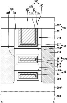
a first high dielectric constant insulating layer formed along the first multi-channel active pattern on the first multi-channel active pattern, wherein the first high dielectric constant insulating layer comprises a metal;
a first gate electrode structure comprising a first silicon nitride layer and a first conductive liner, the first silicon nitride layer and the first conductive liner are formed along the first high dielectric constant insulating layer on the first high dielectric constant insulating layer, the first conductive liner being disposed on the first silicon nitride layer;
a second multi-channel active pattern on the substrate in the second region;
a second high dielectric constant insulating layer formed along the second multi-channel active pattern on the second multi-channel active pattern, wherein the second high dielectric constant insulating layer comprises a metal; and
a second gate electrode structure comprising a second conductive liner formed along the second high dielectric constant insulating layer on the second high dielectric constant insulating layer,
wherein the first conductive liner comprises a first titanium nitride (TiN) layer and a first titanium silicon nitride (TiSiN) layer stacked on each other, and
wherein a thickness of the first TiN layer is different from a thickness of the first TiSiN layer.
|