| CPC H01L 29/4236 (2013.01) [H01L 21/32139 (2013.01); H01L 21/823437 (2013.01); H01L 29/401 (2013.01); H01L 29/66621 (2013.01); H01L 29/7825 (2013.01); H10B 12/053 (2023.02); H10B 12/34 (2023.02); H01L 21/31058 (2013.01); H10B 12/00 (2023.02)] | 12 Claims |
|
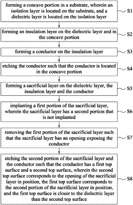
1. A manufacturing method of a semiconductor structure, comprising:
forming a concave portion in a substrate, wherein an isolation layer is located on the substrate, and a dielectric layer is located on the isolation layer;
forming an insulation layer on the dielectric layer and in the concave portion;
forming a conductor on the insulation layer;
etching the conductor such that the conductor is located in the concave portion;
forming a sacrificial layer on the dielectric layer, the insulation layer and the conductor;
implanting a first portion of the sacrificial layer, wherein the sacrificial layer has a second portion that is not implanted;
removing the first portion of the sacrificial layer such that the sacrificial layer has an opening exposing the conductor; and
etching the second portion of the sacrificial layer and the conductor such that the conductor has a first top surface and a second top surface, wherein the second top surface corresponds to the opening of the sacrificial layer in position, the first top surface corresponds to the second portion of the sacrificial layer in position, and the first top surface is closer to the dielectric layer than the second top surface.
|