| CPC H01L 29/41733 (2013.01) [H01L 27/127 (2013.01); H01L 29/66969 (2013.01); H01L 29/78618 (2013.01); H01L 29/78633 (2013.01); H10K 59/1216 (2023.02); H10K 59/126 (2023.02); H10K 59/131 (2023.02); H01L 21/44 (2013.01); H01L 29/7869 (2013.01)] | 10 Claims |
|
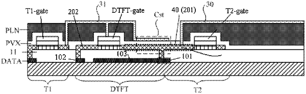
1. An array substrate, the array substrate is an OLED array substrate; and a sub-pixel of the array substrate includes a pixel driving circuit, wherein the pixel driving circuit comprises:
a driving transistor, and an organic light emitting diode connected to a source electrode of the driving transistor; and a drain electrode of the driving transistor is connected to a drain signal line, and the source electrode of the driving transistor is connected to a first electrode of the organic light emitting diode;
a first switching transistor, a second switching transistor, and a storage capacitor, wherein a drain electrode of the first switching transistor is connected to a data line, a source electrode of the first switching transistor is connected to a gate electrode of the driving transistor, and a gate electrode of the first switching transistor is connected to a first gate line; a gate electrode of the second switching transistor is connected to a second gate line, a source electrode of the second switching transistor is connected to a sensing signal line, and a drain electrode of the second switching transistor is connected to the source electrode of the driving transistor; one end of the storage capacitor is connected to the gate electrode of the driving transistor, and the other end is connected to the source electrode of the driving transistor,
wherein the source electrode of the first switching transistor is connected to the gate electrode of the driving transistor through a connection portion,
wherein the first electrode is a transparent electrode; and the connection portion is made of a same material and located in a same layer as the first electrode.
|