| CPC H01L 29/1054 (2013.01) [H01L 21/26506 (2013.01); H01L 21/26586 (2013.01); H01L 29/66545 (2013.01); H01L 29/66636 (2013.01); H01L 29/66659 (2013.01); H01L 29/7848 (2013.01); H01L 29/161 (2013.01); H01L 29/165 (2013.01)] | 10 Claims |
|
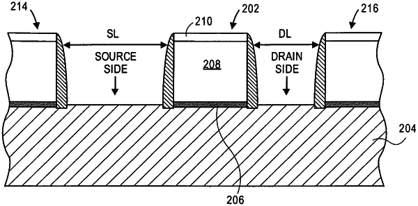
1. A semiconductor device comprising:
a gate stack disposed on a substrate, the substrate having a first lattice constant, the gate stack having a gate electrode;
a source region and a drain region formed on opposite sides of the gate stack;
a channel region disposed beneath the gate stack and between the source region and the drain region, wherein the source region is disposed in a first recess having a first depth and the drain region disposed in a second recess having a second depth, the first recess deeper than the second recess, wherein a portion of the first recess is beneath the gate electrode of the gate stack, and a portion of the second recess is beneath the gate electrode of the gate stack, wherein the portion of the first recess extends laterally further beneath the gate electrode than the portion of the second recess, and wherein the portion of the first recess does not vertically overlap the portion of the second recess, and
wherein a semiconductor material having a second lattice constant different than the first lattice constant is disposed in the first recess and the second recess; and
a source side structure disposed over the substrate wherein the source side structure is spaced apart from the gate stack by a first distance, and a drain side structure disposed on the substrate, wherein the drain side structure is spaced apart from the stack by a second distance, wherein the first distance is greater than the second distance.
|