| CPC H01L 27/15 (2013.01) [H01L 33/382 (2013.01); H01L 33/44 (2013.01); H01L 33/505 (2013.01); H01L 33/62 (2013.01); H01L 2933/0016 (2013.01); H01L 2933/0025 (2013.01); H01L 2933/0066 (2013.01)] | 14 Claims |
|
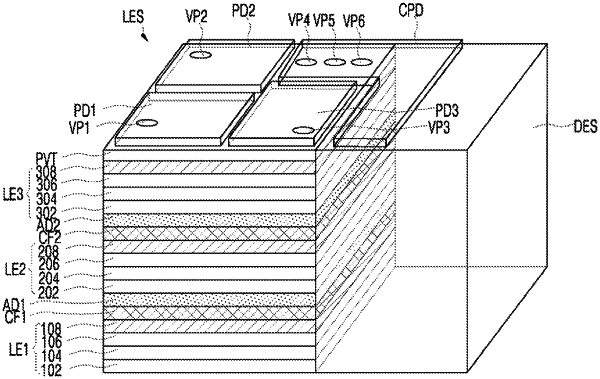
1. A light emitting apparatus comprising:
a light emitting structure including a plurality of light emitting parts comprising a first light emitting part, a second light emitting part, and a third light emitting part each including a first-type semiconductor layer, an active layer, and a second-type semiconductor layer;
a dielectric structure disposed outside the light emitting; and
a plurality of pads disposed on a first surface of the light emitting structure and electrically coupled with the light emitting parts, the pads comprising:
a first pad electrically coupled with the second-type semiconductor layer of the first light emitting part;
a second pad electrically coupled with the second-type semiconductor layer of the second light emitting part;
a third pad electrically coupled with the second-type semiconductor layer of the third light emitting part; and
a common pad electrically coupled with the first-type semiconductor layers of the first, second, and third light emitting parts, the common pad comprising:
a first portion covering at least a portion of the first light emitting part and having a first width in a first direction; and
a second portion extending from the first portion to the first surface of the dielectric structure and having a second width greater than the first width in the first direction,
wherein outer sidewalls of the pads are disposed in a region defined by the light emitting structure and the dielectric structure,
wherein one of the pads extends from the first surface of the light emitting structure to be disposed on a first surface of the dielectric structure, and
wherein the common pad vertically overlaps at least a portion of each of the first light emitting part, the second light emitting part, and the third light emitting part.
|