| CPC H01L 27/124 (2013.01) [G02F 1/13458 (2013.01); H01L 24/05 (2013.01); H01L 24/06 (2013.01); H01L 24/81 (2013.01); H05K 1/111 (2013.01); H01L 2224/05552 (2013.01); H01L 2224/06152 (2013.01); H01L 2224/81132 (2013.01); H01L 2924/3511 (2013.01); H05K 1/189 (2013.01); H05K 2201/09381 (2013.01); H05K 2201/09418 (2013.01); H05K 2201/09427 (2013.01); H05K 2201/09709 (2013.01); H05K 2201/09954 (2013.01); H05K 2201/10128 (2013.01); H05K 2203/166 (2013.01); H10K 59/131 (2023.02); Y02P 70/50 (2015.11); Y10T 29/49005 (2015.01)] | 38 Claims |
|
1. An electronic device, comprising:
a substrate;
a plurality of pixels on the substrate, wherein each of the pixels comprises a thin film transistor and an organic light emitting diode;
a plurality of data lines on the substrate, wherein each of the data lines is electrically connected to some of the thin film transistors;
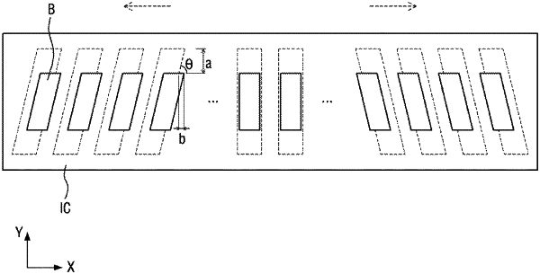
a plurality of first pads arranged side-by-side on the substrate,
wherein:
two of the first pads are inclined with other two of the first pads, and symmetrically arranged with the other two of the first pads;
an integrated circuit having a plurality of bumps is disposed on the first pads; and
a plurality of second pads are arranged outside the intergraded circuit on the substrate.
|