| CPC H01L 25/18 (2013.01) [H01L 21/4857 (2013.01); H01L 21/568 (2013.01); H01L 23/3128 (2013.01); H01L 23/367 (2013.01); H01L 23/49816 (2013.01); H01L 23/5383 (2013.01); H01L 23/5389 (2013.01)] | 20 Claims |
|
1. A method of forming a semiconductor device, the method comprising:
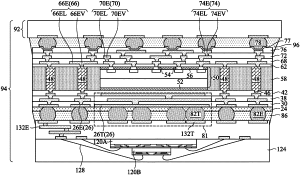
forming a first interconnect structure over a carrier, the first interconnect structure comprising first conductive elements embedded in dielectric layers;
forming a thermal dissipation block over the carrier, the thermal dissipation block comprising second conductive elements embedded in the dielectric layers, wherein forming the thermal dissipation block is simultaneous with forming the first interconnect structure;
forming metal posts over the first interconnect structure;
attaching a first integrated circuit die over the first interconnect structure and the thermal dissipation block;
removing the carrier;
attaching a semiconductor package to the first interconnect structure and the thermal dissipation block using first electrical connectors and thermal dissipation connectors; and
forming external electrical connectors, the external electrical connectors being configured to transmit each external electrical connection into the semiconductor device, the thermal dissipation block being electrically isolated from external electrical connection.
|