| CPC H01L 25/167 (2013.01) [H01L 33/54 (2013.01); H01L 33/60 (2013.01); G09G 3/32 (2013.01); G09G 2310/0267 (2013.01); G09G 2310/0275 (2013.01)] | 20 Claims |
|
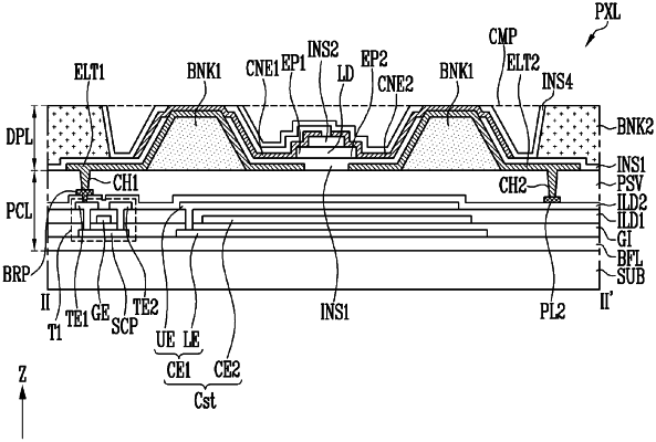
1. A display device comprising:
a substrate including pixels;
a first electrode and a second electrode spaced apart from each other;
light emitting elements disposed between the first electrode and the second electrode;
an insulation layer disposed on the light emitting elements;
a first bank overlapping the first electrode and the second electrode;
a first area overlapping the first bank; and
a second area excluding the first area,
wherein the insulation layer is further disposed on a portion of the first bank and includes an opening on an upper surface of the first bank exposing the first area.
|