| CPC H01L 25/0753 (2013.01) [H01L 24/08 (2013.01); H01L 24/32 (2013.01); H01L 24/73 (2013.01); H01L 25/167 (2013.01); H01L 25/18 (2013.01); H01L 33/60 (2013.01); H01L 33/0008 (2013.01); H01L 33/0093 (2020.05); H01L 33/38 (2013.01); H01L 2224/08225 (2013.01); H01L 2224/32225 (2013.01)] | 17 Claims |
|
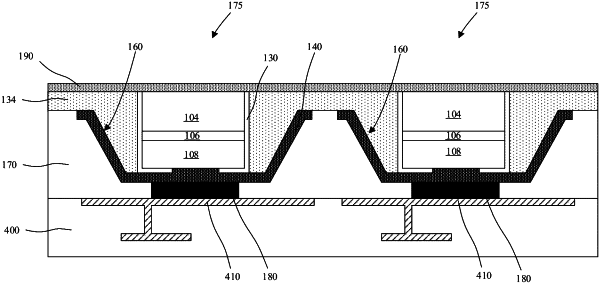
1. A light emitting structure comprising:
a substrate including a top bonding surface including a top surface dielectric bonding layer and an array of electrode pads;
an emission layer stack-up hybrid bonded to the top bonding surface of the substrate, the emission layer stack-up including:
an array of light emitting diodes (LEDs);
an array of reflective metal layers, wherein each reflective metal layer spans laterally around and underneath a corresponding LED, and each reflective metal layer is in electrical contact with a bottom surface of a corresponding LED;
a dielectric bonding layer spanning underneath the array of LEDs; and
an array of bond posts directly connected to the array of reflective metal layers and extending through the dielectric bonding layer;
wherein each bond post is metal-metal bonded with an electrode pad of the substrate, and the dielectric bonding layer is directly bonded with the top surface dielectric bonding layer of the substrate.
|