| CPC H01L 25/0652 (2013.01) [H01L 23/16 (2013.01); H01L 23/3128 (2013.01); H01L 23/3135 (2013.01); H01L 23/3675 (2013.01); H01L 23/562 (2013.01); H01L 2225/06513 (2013.01); H01L 2225/06541 (2013.01); H01L 2225/06586 (2013.01); H01L 2225/06589 (2013.01)] | 20 Claims |
|
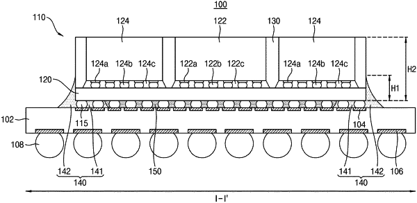
1. A package structure, comprising:
a lower substrate;
substrate connection terminals on the lower substrate;
a semiconductor package on the substrate connection terminals, the semiconductor package including a package substrate and an encapsulant covering the package substrate; and
a first underfill and a second underfill between the lower substrate and the semiconductor package, the first underfill including:
an inner portion overlapping the semiconductor package in a vertical direction, the inner portion covering at least one of the substrate connection terminals, and
an outer portion not overlapping the semiconductor package in the vertical direction.
|