| CPC H01L 25/0652 (2013.01) [H01L 23/49822 (2013.01); H01L 25/50 (2013.01)] | 19 Claims |
|
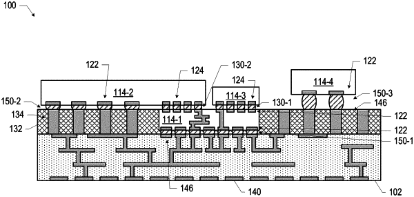
1. A microelectronic assembly, comprising:
a first redistribution layer;
a first die above the redistribution layer, the first die having a top side and a bottom side, and a first sidewall and a second sidewall between the top side and the bottom side, the second sidewall laterally opposite the first sidewall, and the first die comprising a plurality of through substrate vias;
a first conductive pillar laterally spaced apart from the first sidewall of the first die;
a second conductive pillar laterally spaced apart from the second sidewall of the first die;
a mold material on the first redistribution layer and laterally surrounding the first die, the first conductive pillar, and the second conductive pillar, the mold material in contact with the first conductive pillar, the second conductive pillar, the first sidewall of the first die, and the second sidewall of the first die;
a second redistribution layer having a top surface and a bottom surface, the bottom surface on the first conductive pillar, on the second conductive pillar, on the mold material, and over the first die;
a second die coupled to the top surface of the second redistribution layer, the second die vertically over the first die; and
a third die coupled to the top surface of the second redistribution layer, the third die vertically over the first die, and the third die laterally spaced apart from the second die, wherein the first die electrically couples the second die to the third die.
|