| CPC H01L 25/0652 (2013.01) [H01L 21/52 (2013.01); H01L 21/56 (2013.01); H01L 23/3128 (2013.01); H01L 23/42 (2013.01); H01L 23/5383 (2013.01); H01L 23/5384 (2013.01); H01L 23/5385 (2013.01); H01L 23/5389 (2013.01); H01L 25/50 (2013.01)] | 20 Claims |
|
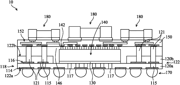
1. A method of forming a package structure, comprising:
forming a plurality of conductive features in a substrate and protruding from a top surface of the substrate;
etching the top surface of the substrate to form a cavity, wherein the substrate comprises a plurality of thermal vias directly under a bottom surface of the cavity;
forming at least one first electronic device in the cavity of the substrate, wherein the first electronic device is thermally coupled to the plurality of thermal vias;
forming an encapsulating material in the cavity, so that the encapsulating material extends along sidewalls of the first electronic device and covers a surface of the first electronic device opposite the bottom surface of the cavity; and
forming an insulating layer having a redistribution layer (RDL) structure over the encapsulating material, wherein the RDL structure is electrically connected to the first electronic device, wherein a bottom surface of the insulating layer is in direct contact with a top surface of the encapsulating material and a top surface of the plurality of conductive features.
|