| CPC H01L 24/20 (2013.01) [H01L 24/73 (2013.01); H01L 25/105 (2013.01); H01L 2224/2101 (2013.01); H01L 2224/2105 (2013.01); H01L 2224/221 (2013.01); H01L 2224/73101 (2013.01); H01L 2225/1035 (2013.01); H01L 2225/1041 (2013.01); H01L 2225/1058 (2013.01)] | 20 Claims |
|
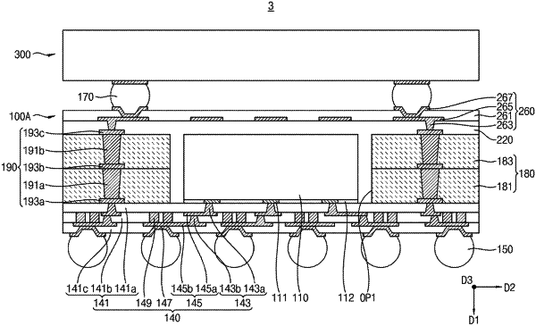
1. A semiconductor package comprising:
a semiconductor chip;
a lower redistribution layer on a lower surface of the semiconductor chip, the lower redistribution layer comprising an insulating layer, a redistribution pattern on the insulating layer, a via connected to an upper surface of the redistribution pattern and extending through the insulating layer in a vertical direction, an under bump metal (UBM) disposed on a lower surface of the redistribution pattern, and a post disposed on the upper surface of the redistribution pattern, the post vertically overlaps with the UBM;
a mold layer on the lower redistribution layer, the mold layer surrounding a lateral side surface of the semiconductor chip; and
a connecting terminal connected to the UBM,
wherein the UBM comprises a first section having an upper surface directly contacting the redistribution pattern, and a second section having an upper surface directly contacting the insulating layer,
wherein the post has a ring shape having an inner surface and an outer surface when viewed in a top view,
wherein, when viewed in the top view a maximum width of the inner surface is less than maximum width of an upper surface of the first section, and a maximum width of the outer surface is greater than the maximum width of the upper surface of the first section.
|