| CPC H01L 24/08 (2013.01) [H01L 24/80 (2013.01); H01L 25/0657 (2013.01); H01L 25/18 (2013.01); H01L 25/50 (2013.01); H01L 2224/08145 (2013.01); H01L 2224/80895 (2013.01); H01L 2224/80896 (2013.01); H01L 2924/1431 (2013.01); H01L 2924/14511 (2013.01)] | 20 Claims |
|
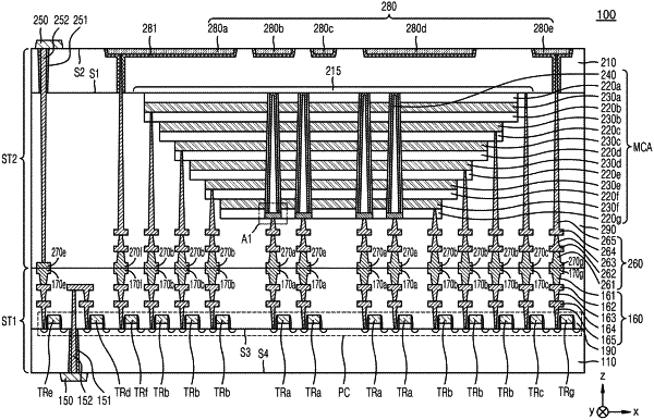
1. A memory device, comprising:
a first structure; and
a second structure on the first structure, wherein:
the first structure includes:
a first substrate;
a peripheral circuit on the first substrate;
a first insulating layer covering the first substrate and the peripheral circuit; and
a first bonding pad on the first insulating layer,
the second structure includes:
a second substrate;
a memory cell array on a first surface of the second substrate;
a second insulating layer directly contacting and covering the first surface of the second substrate and the memory cell array;
a conductive pattern at least partially recessed from a second surface of the second substrate; and
a second bonding pad on the second insulating layer,
the first bonding pad is in contact with the second bonding pad, and
the conductive pattern is spaced apart from the second insulating layer.
|