| CPC H01L 23/66 (2013.01) [H01L 23/3672 (2013.01); H01L 23/3733 (2013.01); H01L 23/49822 (2013.01); H01L 23/49838 (2013.01); H01L 24/16 (2013.01); H01Q 1/02 (2013.01); H01Q 1/2283 (2013.01); H01L 2223/6677 (2013.01); H01L 2224/16227 (2013.01); H01L 2924/01029 (2013.01); H01L 2924/0103 (2013.01); H01L 2924/01047 (2013.01); H01L 2924/01049 (2013.01); H01L 2924/0105 (2013.01); H01L 2924/01051 (2013.01); H01L 2924/01083 (2013.01); H01L 2924/014 (2013.01); H01L 2924/18161 (2013.01)] | 12 Claims |
|
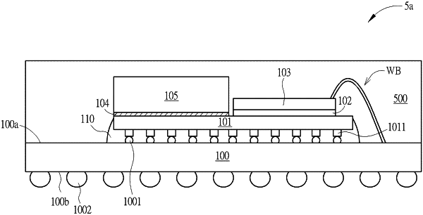
1. A semiconductor package, comprising:
a base comprising a top surface and a bottom surface that is opposite to the top surface;
a first semiconductor chip mounted on the top surface of the base in a flip-chip manner;
a second semiconductor chip stacked on the first semiconductor chip and electrically coupled to the base by at least one connecting element;
an in-package heat dissipating element comprising a dummy silicon die disposed over a top surface of the first semiconductor chip by using a high-thermal conductivity die attach film; and
a molding compound encapsulating the first semiconductor chip, the second semiconductor chip, and the in-package heat dissipating element,
wherein the second semiconductor chip and the in-package heat dissipating element are attached onto the top surface of the first semiconductor chip in a side-by-side manner.
|