| CPC H01L 23/552 (2013.01) [H01L 21/4853 (2013.01); H01L 21/565 (2013.01); H01L 23/3128 (2013.01); H01L 23/49816 (2013.01); H01L 23/5383 (2013.01); H01L 24/16 (2013.01); H01L 24/48 (2013.01); H01L 24/73 (2013.01); H01L 25/0652 (2013.01); H01L 2224/16227 (2013.01); H01L 2224/32145 (2013.01); H01L 2224/32225 (2013.01); H01L 2224/48091 (2013.01); H01L 2224/48227 (2013.01); H01L 2224/73253 (2013.01); H01L 2224/73265 (2013.01); H01L 2225/0651 (2013.01); H01L 2225/06517 (2013.01); H01L 2225/06558 (2013.01); H01L 2924/15192 (2013.01); H01L 2924/15311 (2013.01); H01L 2924/3025 (2013.01)] | 20 Claims |

|
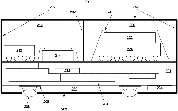
1. An apparatus, comprising:
a substrate comprising substrate conductive traces, a substrate top side, a substrate bottom side, and substrate sidewalls between the substrate top side and the substrate bottom side;
a first semiconductor device coupled to the substrate conductive traces;
a second semiconductor device coupled to the substrate conductive traces;
an upper encapsulant that encapsulates the first semiconductor device, the second semiconductor device, and a portion of the substrate top side;
a lower encapsulant that encapsulates a portion of the substrate bottom side;
an electromagnetic interference (EMI) shield that covers the upper encapsulant and the substrate sidewalls; and
an internal shield component comprising an internal shield component first lateral side and an internal shield component second lateral side that pass through the upper encapsulant and couple the EMI shield to a ground portion of the substrate conductive traces;
wherein the internal shield component second lateral side is opposite the internal shield component first lateral side; and
wherein the upper encapsulant contacts the internal shield component first lateral side and the internal shield component second lateral side.
|