| CPC H01L 23/5389 (2013.01) [H01L 23/5286 (2013.01); H01L 24/13 (2013.01); H01L 24/17 (2013.01); H01L 24/19 (2013.01); H01L 24/20 (2013.01); H01L 24/24 (2013.01); H01L 24/25 (2013.01); H01L 24/73 (2013.01); H01L 25/105 (2013.01); H01L 21/486 (2013.01); H01L 23/3128 (2013.01); H01L 23/5384 (2013.01); H01L 23/562 (2013.01); H01L 2224/04105 (2013.01); H01L 2224/12105 (2013.01); H01L 2224/13024 (2013.01); H01L 2224/17181 (2013.01); H01L 2224/24105 (2013.01); H01L 2224/24226 (2013.01); H01L 2224/25171 (2013.01); H01L 2224/32145 (2013.01); H01L 2224/48091 (2013.01); H01L 2224/48227 (2013.01); H01L 2224/73101 (2013.01); H01L 2224/73209 (2013.01); H01L 2224/73259 (2013.01); H01L 2224/73265 (2013.01); H01L 2224/73267 (2013.01); H01L 2224/92244 (2013.01); H01L 2225/1035 (2013.01); H01L 2225/1058 (2013.01); H01L 2225/1094 (2013.01); H01L 2924/15311 (2013.01); H01L 2924/181 (2013.01)] | 20 Claims |
|
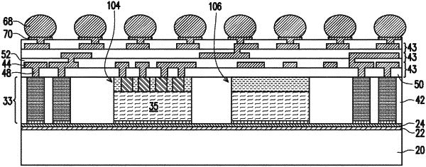
1. A semiconductor structure, comprising:
a functional die on a first polymer layer, wherein the functional die comprises a first insulating layer over a first substrate;
a dummy die on the first polymer layer, wherein the dummy die comprises a second insulating layer overlying a second substrate, wherein the dummy die is free of active devices;
a molding compound along sidewalls of the functional die and the dummy die; and
a redistribution structure over the functional die, the dummy die, and the molding compound, the redistribution structure comprising a first conductive line electrically coupled to the functional die, wherein the redistribution structure comprises a first external contact on a side opposite the functional die.
|