| CPC H01L 23/5384 (2013.01) [H01L 23/5386 (2013.01); H01L 25/0655 (2013.01)] | 7 Claims |
|
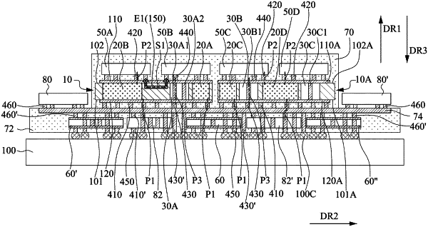
1. An electronic package comprising:
a semiconductor substrate comprising a first active region and a first passive region separated from the first active region, wherein the first active region is configured to regulate a power signal, and the first passive region is configured to transmit a data signal,
wherein the first active region comprises a conductive through via having a resistance lower than a resistance of a conductive through via of the first passive region,
wherein the first active region comprises a plurality of the conductive through vias, and
wherein a size of the conductive through via of the first active region is different from a size of the conductive through via of the first passive region.
|