| CPC H01L 23/5383 (2013.01) [H01L 21/4857 (2013.01); H01L 23/552 (2013.01); H01L 24/16 (2013.01); H01L 24/73 (2013.01); H01L 24/92 (2013.01); H01L 25/105 (2013.01); H01L 25/50 (2013.01); H01Q 1/22 (2013.01); H01L 2224/16227 (2013.01); H01L 2224/73103 (2013.01); H01L 2224/9211 (2013.01)] | 14 Claims |

|
1. A wafer stacking structure comprising:
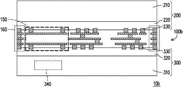
an interlayer having a first surface and a second surface opposite to the first surface and comprising a dielectric material layer and a redistribution layer embedded in the dielectric material layer;
a first wafer disposed on the first surface of the interlayer, wherein the first wafer comprises a plurality of first conductive contacts, and the first conductive contacts contact the redistribution layer; and
a second wafer disposed on the second surface of the interlayer, wherein the second wafer comprises a plurality of second conductive contacts, and the second conductive contacts contact the redistribution layer,
wherein the second wafer is electrically connected to the first wafer through the redistribution layer of the interlayer, the first conductive contacts are columnar metals protruding from the first wafer, and the second conductive contacts are columnar metals protruding from the second wafer,
wherein each of the first conductive contacts does not overlap with anyone of the second contacts in a normal direction of the wafer stacking structure,
wherein the interlayer further comprises a shielding structure and an antenna structure, the shielding structure is embedded in the interlayer to shield a radiation signal from the second wafer, and the antenna structure is disposed on a side of the interlayer to emit and/or receive a signal.
|