| CPC H01L 23/528 (2013.01) [H10B 43/27 (2023.02)] | 12 Claims |
|
1. A method of manufacturing a semiconductor device, the method comprising:
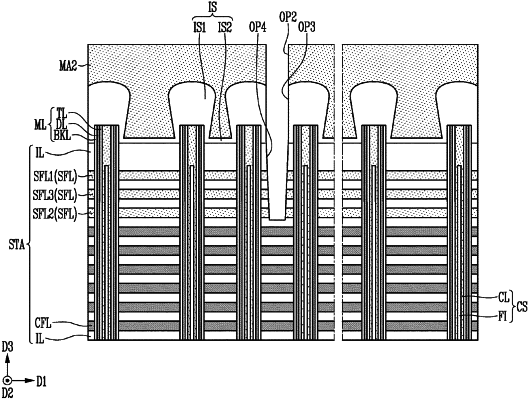
forming a stack structure including a cell sacrificial layer, a select sacrificial layer, and a stack insulating layer, which overlap with each other;
forming a first opening exposing the select sacrificial layer;
removing the select sacrificial layer through the first opening;
forming a first part of a filling sacrificial layer in an empty space formed by removing the select sacrificial layer;
forming a second opening exposing the first part of the filling sacrificial layer and the cell sacrificial layer; and
removing the first part of the filling sacrificial layer and the cell sacrificial layer.
|