| CPC H01L 23/5226 (2013.01) [H01L 23/53238 (2013.01); H01L 23/53252 (2013.01); H01L 23/53266 (2013.01); H01L 29/45 (2013.01)] | 15 Claims |
|
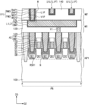
1. A semiconductor device comprising:
a substrate;
a first interlayer insulating layer on the substrate;
a lower interconnection line in the first interlayer insulating layer;
an etch stop layer on the first interlayer insulating layer and the lower interconnection line;
a second interlayer insulating layer on the etch stop layer; and
an upper interconnection line in the second interlayer insulating layer, the upper interconnection line including a via portion extending through the etch stop layer and contacting the lower interconnection line,
wherein the via portion comprises a barrier pattern and a conductive pattern on the barrier pattern,
wherein the barrier pattern comprises a first portion that is between the conductive pattern and the second interlayer insulating layer and a second portion that is between the conductive pattern and the lower interconnection line,
wherein the first portion of the barrier pattern has a first nitrogen concentration, the second portion of the barrier pattern has a second nitrogen concentration, and the first nitrogen concentration is greater than the second nitrogen concentration, and
wherein the first portion of the barrier pattern has a first thickness, and the second portion of the barrier pattern has a second thickness, and the first thickness is greater than the second thickness.
|