| CPC H01L 23/49822 (2013.01) [H01L 23/147 (2013.01); H01L 23/49816 (2013.01); H01L 23/49838 (2013.01); H01L 24/17 (2013.01); H01L 25/0652 (2013.01); H01L 2224/17104 (2013.01)] | 20 Claims |
|
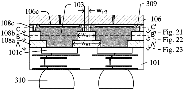
15. A semiconductor structure, comprising:
a first substrate including a first plurality of conductive pads that are laterally spaced apart from one another on the first substrate;
a second substrate including a second plurality of conductive pads that are laterally spaced apart from one another on the second substrate;
a first plurality of conductive bumps disposed on the first plurality of conductive pads, respectively; and
a multi-tiered solder-resist structure vertically separating the first substrate and the second substrate and laterally separating adjacent conductive bumps of the first plurality of conductive bumps from one another, the multi-tiered solder-resist structure including conductive bump openings having different widths at different heights over the first substrate and through which the first plurality of conductive bumps pass such that the multi-tiered solder-resist structure separates the first plurality of conductive bumps from one another;
wherein the multi-tiered solder-resist structure comprises:
a first tier comprising a first dielectric material and including first conductive bump openings defined by inner sidewalls of the first tier, the first tier having a first width measured through the first dielectric material between the inner sidewalls of the first tier; and
a second tier overlying the first tier, the second tier comprising a second dielectric material and including second conductive bump openings defined by inner sidewalls of the second tier, the second tier having a second width measured through the second dielectric material between the inner sidewalls of the second tier; and
a third tier overlying the second tier, the third tier comprising a third dielectric material and including third conductive bump openings defined by inner sidewalls of the third tier, the third tier having a third width measured through the third dielectric material between the inner sidewalls of the third tier;
wherein the first width is greater than the second width, and wherein the second width is greater than third width;
wherein the inner sidewalls of the third tier are directly over a top surface of the second tier, and wherein a top surface of the third tier is above bottom surfaces of the second plurality of conductive pads.
|