| CPC H01L 23/49816 (2013.01) [H01L 21/4853 (2013.01); H01L 21/56 (2013.01); H01L 23/3121 (2013.01); H01L 23/49861 (2013.01); H01L 24/13 (2013.01); H01L 23/5385 (2013.01); H01L 2224/023 (2013.01); H01L 2225/107 (2013.01)] | 20 Claims |
|
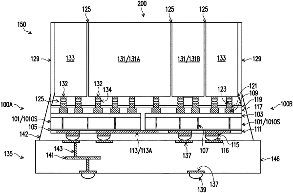
1. A method of forming a semiconductor structure, the method comprising:
placing a first interposer laterally adjacent to a second interposer;
embedding the first interposer and the second interposer in a first molding material;
bonding a first die to the first interposer and the second interposer, wherein a first die connector of the first die is bonded with a first conductive bump at a first side of the first interposer, and a second die connector of the first die is bonded with a second conductive bump at a first side of the second interposer;
forming an underfill material between the first die and the first interposer; and
forming a second molding material around the first die, wherein the first molding material contacts and extends along the second molding material.
|