| CPC H01L 23/433 (2013.01) [H01L 23/13 (2013.01); H01L 23/4334 (2013.01); H01L 23/473 (2013.01); H01L 23/49568 (2013.01); H01L 23/49861 (2013.01); H01L 25/0657 (2013.01); H01L 23/24 (2013.01); H01L 2224/33 (2013.01)] | 18 Claims |
|
1. A semiconductor package comprising:
a first cover coupled to a first substrate, the first substrate coupled to a first die;
a first cooling system positioned between an inner face of the first substrate and an outer face of the first cover;
a second cover coupled to a second substrate, the second substrate coupled to a second die;
a second cooling system positioned between an inner face of the second substrate and an outer face of the second cover; and
a spacer coupled between the first die and the second die;
wherein the first cooling system and the second cooling system each comprise a flow control device configured to induce turbulent flow of a cooling medium passing through the first cooling system and the second cooling system;
wherein the first substrate and the second substrate are configured to contact the cooling medium; and
wherein each substrate of the semiconductor package is directly coupled to one of the first cover or the second cover.
|
|
9. A semiconductor package comprising:
a first cover coupled to a first substrate, the first substrate coupled to a first die;
a first cooling system comprised in the first cover and positioned between an inner face of the first substrate and an outer face of the first cover;
a second cover coupled to a second substrate, the second substrate coupled to a second die;
a second cooling system comprised in the second cover and positioned between an inner face of the second substrate and an outer face of the second cover; and
a spacer coupled between the first die and the second die;
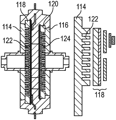
wherein the first cooling system and the second cooling system each comprise a heat slug with fins; and
wherein the first substrate and the second substrate are configured to contact a cooling medium configured to pass through the first cooling system and the second cooling system.
|
|
13. A semiconductor package comprising:
a first cover coupled to a first substrate, the first substrate coupled to a first die;
a first cooling system comprised in the first cover and positioned between an inner face of the first substrate and an outer face of the first cover;
a second cover coupled to a second substrate, the second substrate coupled to a second die;
a second cooling system comprised in the second cover and positioned between an inner face of the second substrate and an outer face of the second cover; and
a spacer coupled between the first die and the second die;
wherein the first cooling system and the second cooling system each comprise a flow control device configured to induce turbulent flow of a cooling medium passing through the first cooling system and the second cooling system;
wherein the first substrate and the second substrate are configured to contact the cooling medium; and
wherein each substrate of the semiconductor package is directly coupled to one of the first cover or the second cover.
|