| CPC H01L 22/12 (2013.01) [G03F 7/70633 (2013.01); G03F 7/70683 (2013.01); H01L 22/30 (2013.01); H01L 23/544 (2013.01); H01L 2223/54426 (2013.01)] | 26 Claims |
|
1. A product, comprising:
a semiconductor substrate;
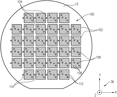
at least first and second thin-film layers disposed on the substrate and patterned to define a matrix of dies, which are separated by scribe lines and contain active areas circumscribed by the scribe lines; and
a plurality of overlay targets formed in the first and second thin-film layers within each of the active areas, each overlay target having dimensions no greater than 10 μm×10 μm in a plane parallel to the substrate and comprising:
a first linear grating formed in the first thin-film layer and having a first grating vector; and
a second linear grating formed in the second thin-film layer, in proximity to the first linear grating, and having a second grating vector parallel to the first grating vector.
|