| CPC H01L 21/823431 (2013.01) [H01L 21/823418 (2013.01); H01L 21/823468 (2013.01); H01L 29/6681 (2013.01)] | 20 Claims |
|
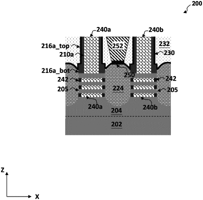
1. A method, comprising:
forming a dummy gate stack over a semiconductor layer;
forming a spacer layer over the semiconductor layer, wherein the spacer layer comprising a vertical part extending along an upper portion of the dummy gate stack and a horizontal part in direct contact with both the semiconductor layer and a lower portion of the dummy gate stack;
treating the spacer layer to form a step sidewall for the vertical part of the spacer layer, wherein a bottom portion of the vertical part of the spacer layer has a greater thickness than a top portion of the vertical part of the spacer layer;
etching portions of the treated spacer layer, such that remaining portions of the treated spacer layer are disposed along sidewalls of the dummy gate stack; and
forming a source/drain (S/D) feature in the semiconductor layer adjacent to the remaining portions of the treated spacer layer.
|