| CPC H01L 21/76897 (2013.01) [H01L 21/31116 (2013.01); H01L 21/76831 (2013.01); H01L 21/76879 (2013.01); H01L 29/66545 (2013.01)] | 20 Claims |
|
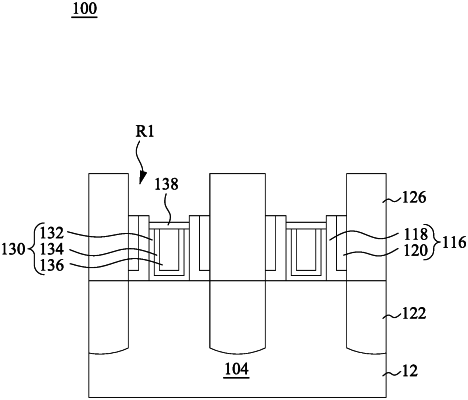
1. A method comprising:
depositing a dielectric cap over a gate structure;
forming a source/drain contact over a source/drain region adjacent to the gate structure;
oxidizing a top portion of the dielectric cap to form an oxidized top portion while a bottom portion of the dielectric cap that is between the oxidized top portion and the gate structure remains un-oxidized, wherein a top surface of the bottom portion is directly connected to a bottom surface of the oxidized top portion;
after oxidizing the top portion of the dielectric cap, depositing an etch stop layer over the oxidized top portion of the dielectric cap and an interlayer dielectric (ILD) layer over the etch stop layer;
etching the ILD layer and the etch stop layer to form a via opening extending though the ILD layer and the etch stop layer; and
filling a source/drain via in the via opening.
|