| CPC H01L 21/76877 (2013.01) [H01L 21/02164 (2013.01); H01L 21/0217 (2013.01); H01L 21/31111 (2013.01); H01L 21/32055 (2013.01); H01L 21/32135 (2013.01); H01L 21/76802 (2013.01); H10B 41/27 (2023.02); H10B 43/27 (2023.02)] | 19 Claims |
|
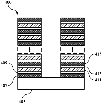
1. A method of forming a semiconductor structure, the method comprising:
forming a first silicon oxide layer overlying a semiconductor substrate;
forming a first silicon layer overlying the first silicon oxide layer;
forming a silicon nitride layer overlying the first silicon layer;
forming a second silicon layer overlying the silicon nitride layer;
forming a second silicon oxide layer overlying the second silicon layer;
removing the silicon nitride layer;
removing the first silicon layer and the second silicon layer; and
forming a metal layer between each of the first silicon oxide layer and the second silicon oxide layer.
|