| CPC H01L 21/76829 (2013.01) [C23F 1/12 (2013.01); H01L 21/02178 (2013.01); H01L 21/76802 (2013.01); H01L 23/5226 (2013.01); H01L 23/53209 (2013.01); H01L 23/53295 (2013.01)] | 20 Claims |
|
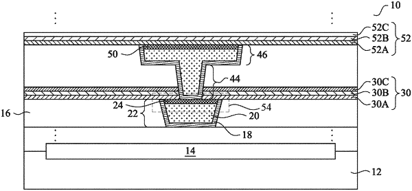
1. A method comprising:
forming a first conductive feature over a substrate;
forming an amorphous metal cap on the first conductive feature;
depositing a dielectric layer over the amorphous metal cap;
etching the dielectric layer to form an opening; and
filling the opening with a conductive material to form a second conductive feature contacting the amorphous metal cap.
|