| CPC H01L 21/76224 (2013.01) [H01L 21/02164 (2013.01); H01L 21/0217 (2013.01); H01L 21/02359 (2013.01); H01L 21/31144 (2013.01)] | 9 Claims |
|
1. A method for making a high-voltage thick gate oxide, wherein the method comprises the following steps:
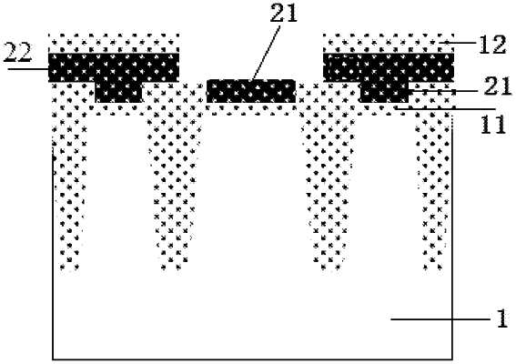
step 1: depositing a pad silicon oxide on a silicon substrate and depositing a pad silicon nitride on the pad silicon oxide; then performing photolithography and etching to form trenches on the silicon substrate; then performing silicon oxide filling in the trenches and chemical mechanical polishing to form shallow trench isolations;
step 2: depositing a mask silicon nitride on a silicon wafer and depositing a mask silicon oxide on the mask silicon nitride;
step 3: performing photolithography and etching by using the mask silicon oxide as a hard mask, removing the mask silicon oxide and the mask silicon nitride in a high-voltage thick gate oxide region, and remaining the pad silicon nitride between two shallow trench isolations in the high-voltage thick gate oxide region;
step 4: performing first thermal oxidation growth to passivate shallow trench isolation corners in the high-voltage gate oxide region;
step 5: removing the pad silicon nitride between the two shallow trench isolations in the high-voltage thick gate oxide region;
step 6: performing second thermal oxidation growth to produce a high-voltage thick gate oxide; and
step 7: removing all of the mask silicon nitride and pad silicon nitride.
|