US 11,967,516 B2
Substrate support for chucking of mask for deposition processes
Jrjyan Jerry Chen, Campbell, CA (US); Sanjay D. Yadav, Morgan Hill, CA (US); Tae Kyung Won, San Jose, CA (US); Jun Li, Sunnyvale, CA (US); Shouqian Shao, Fremont, CA (US); and Surendra Kanimihally Setty, San Jose, CA (US)
Assigned to Applied Materials, Inc., Santa Clara, CA (US)
Appl. No. 17/423,689
Filed by Applied Materials, Inc., Santa Clara, CA (US)
PCT Filed Jan. 17, 2020, PCT No. PCT/US2020/014061
§ 371(c)(1), (2) Date Jul. 16, 2021,
PCT Pub. No. WO2020/163060, PCT Pub. Date Aug. 13, 2020.
Claims priority of provisional application 62/801,605, filed on Feb. 5, 2019.
Prior Publication US 2022/0122876 A1, Apr. 21, 2022
Int. Cl. H01T 23/00 (2006.01); C23C 16/04 (2006.01); C23C 16/458 (2006.01); C23C 16/50 (2006.01); H01J 37/32 (2006.01); H01L 21/683 (2006.01); H01L 21/687 (2006.01)
CPC H01L 21/6833 (2013.01) [C23C 16/042 (2013.01); C23C 16/4586 (2013.01); C23C 16/50 (2013.01); H01J 37/32715 (2013.01); H01L 21/68757 (2013.01); H01L 21/68785 (2013.01); H01J 2237/2007 (2013.01); H01J 2237/3321 (2013.01)] 20 Claims
OG exemplary drawing
 
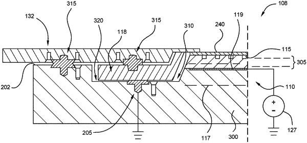
1. A substrate support, comprising:
a substrate receiving surface;
a recessed portion disposed about a periphery of the substrate receiving surface, the recessed portion configured for receipt of a shadow frame;
an electrostatic chuck disposed below the substrate receiving surface; and
a plurality of compressible buttons, each compressible button disposed within a respective opening formed in the recessed portion and forming an electrical circuit with the electrostatic chuck.