US 11,967,507 B2
Tie bar removal for semiconductor device packaging
Richard Te Gan, Chandler, AZ (US); Rushik Prabhudas Tank, Chandler, AZ (US); Zhiwei Gong, Chandler, AZ (US); Burton Jesse Carpenter, Austin, TX (US); and Jinmei Liu, Tianjin (CN)
Assigned to NXP USA, INC., Austin, TX (US)
Filed by NXP USA, INC., Austin, TX (US)
Filed on Dec. 6, 2021, as Appl. No. 17/457,726.
Application 17/457,726 is a division of application No. 16/862,027, filed on Apr. 29, 2020, granted, now 11,222,790.
Claims priority of application No. 201911373697.6 (CN), filed on Dec. 26, 2019.
Prior Publication US 2022/0093416 A1, Mar. 24, 2022
Int. Cl. H01L 21/48 (2006.01); H01L 21/56 (2006.01); H01L 23/31 (2006.01); H01L 23/495 (2006.01)
CPC H01L 21/4842 (2013.01) [H01L 21/4825 (2013.01); H01L 21/565 (2013.01); H01L 23/3114 (2013.01); H01L 23/49503 (2013.01); H01L 23/49548 (2013.01)] 20 Claims
OG exemplary drawing
 
1. A semiconductor device comprising:
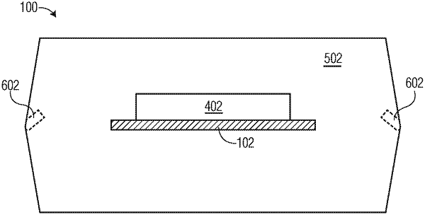
a leadframe having a plurality of conductive leads and a flag;
a semiconductor die attached to the flag of the leadframe; and
a molding compound encapsulating the semiconductor die and a portion of the leadframe, an angled cavity formed in the molding compound at an end of the semiconductor device substantially perpendicular to the flag, the angled cavity formed at an angle different from a plane of the flag.