| CPC H01L 21/02603 (2013.01) [H01L 21/02208 (2013.01); H01L 21/02271 (2013.01); H01L 21/0262 (2013.01)] | 20 Claims |
|
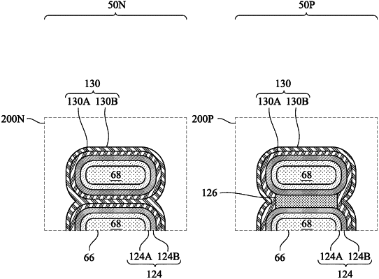
1. A method comprising:
depositing a sacrificial layer around a first nanostructure and a second nanostructure using a non-conformal deposition process, wherein the first nanostructure is disposed over and separated from the second nanostructure by a first recess, and wherein the first nanostructure and the second nanostructure are disposed over a semiconductor substrate in a first device region;
patterning the sacrificial layer, wherein after patterning the sacrificial layer, a remaining portion of the sacrificial layer is disposed in the first recess between the first nanostructure and the second nanostructure;
depositing a first work function tuning layer over the first nanostructure and the second nanostructure;
patterning the first work function tuning layer to remove the first work function tuning layer in the first device region;
removing the remaining portion of the sacrificial layer;
after removing the remaining portion of the sacrificial layer, depositing a second work function tuning layer around the first nanostructure and the second nanostructure; and
depositing a gate fill material over the second work function tuning layer.
|