| CPC H01L 21/02274 (2013.01) [H01L 28/40 (2013.01)] | 20 Claims |
|
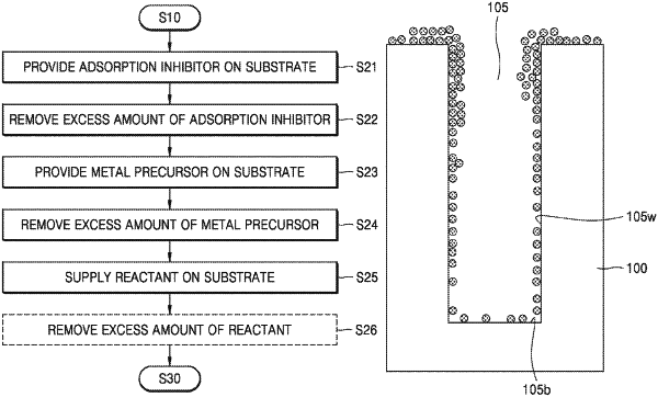
1. A method of forming a material layer, the method comprising:
a deposition cycle comprising:
providing an adsorption inhibitor on a substrate;
purging an excess amount of the adsorption inhibitor;
providing a metal precursor on the substrate;
purging an excess amount of the metal precursor; and
supplying a reactant to form a material layer on the substrate,
wherein the adsorption inhibitor includes a group 15 element or a group 16 element, and
wherein the reactant includes one or more selected from a group consisting of nitrogen (N2), ammonia (NH3), hydrazine (N2H4), diazene (N2H2), N2O, NO, NO2, N2 plasma, NH3 plasma, H2 plasma, and NF3.
|