| CPC H01L 21/02126 (2013.01) [C23C 16/325 (2013.01); H01L 21/02167 (2013.01); H01L 21/02274 (2013.01); H01L 21/02205 (2013.01); H01L 21/02211 (2013.01); H01L 21/02216 (2013.01)] | 13 Claims |
|
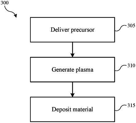
1. A method of forming a silicon-and-carbon-containing material, the method comprising:
flowing a silicon-oxygen-and-carbon-containing precursor into a processing region of a semiconductor processing chamber, wherein a substrate is housed within the processing region of the semiconductor processing chamber, and wherein the silicon-oxygen-and-carbon-containing precursor characterized by a carbon-to-oxygen ratio that is less than 4:1;
forming a plasma within the processing region of the silicon-oxygen-and-carbon-containing precursor, wherein the plasma is formed at a frequency below 15 MHz; and
depositing a silicon-and-carbon-containing material on the substrate, wherein the silicon-and-carbon-containing material as-deposited is characterized by a dielectric constant below 3.5, wherein a deposition rate of the silicon-and-carbon-containing material is greater than 500 Å/min, and wherein the silicon-and-carbon-containing material as-deposited is characterized by a methyl incorporation less than 2.5%.
|