| CPC G11C 16/08 (2013.01) [G11C 5/06 (2013.01); G11C 16/24 (2013.01); G11C 16/26 (2013.01)] | 12 Claims |
|
1. A semiconductor memory device comprising:
a memory cell array including a plurality of memory cells;
a row decoder connected to the memory cell array through word lines;
a plurality of page buffers connected to the memory cell array through bit lines; and
a voltage switching circuit configured to decode an operation voltage and transmit the decoded operation voltage to the row decoder,
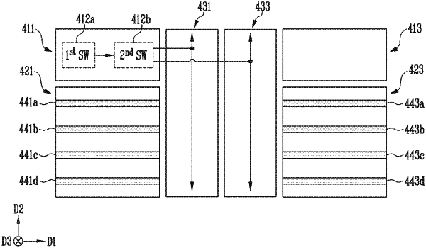
wherein the plurality of page buffers are formed in a first under cell region among first and second under cell regions, the first and second under cell regions being adjacent to each other in a first direction under the memory cell array,
wherein at least a portion of the voltage switching circuit is formed in an under slim region that is adjacent to the first under cell region and the second under cell region in a second direction,
wherein the voltage switching circuit includes a first switch circuit and a second switch circuit, and
wherein the first switch circuit is formed in the second under cell region, and the second switch circuit is formed in the under slim region.
|