| CPC G11C 13/0059 (2013.01) [G11C 13/0007 (2013.01); G11C 13/0038 (2013.01); G11C 13/004 (2013.01); G11C 13/0069 (2013.01); H04L 9/3278 (2013.01); H10B 63/80 (2023.02); H10N 70/24 (2023.02); H10N 70/801 (2023.02); H10N 70/841 (2023.02); G11C 2013/0045 (2013.01); G11C 2013/0078 (2013.01); G11C 2013/0088 (2013.01)] | 19 Claims |
|
1. An electronic device, comprising:
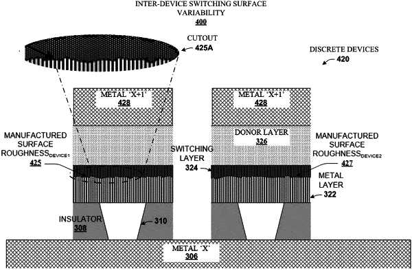
an array of two-terminal resistive switching memory;
a memory controller operably coupled to the array of two-terminal resistive switching memory and configured to select a subset of two-terminal memory devices of the array for a physical unclonable feature (PUF) write operation; and
a sensing circuit configured to measure an electrical characteristic of a two-terminal memory device of the array in response to the PUF write operation; and wherein the PUF write operation is characterized by:
the memory controller selects a first two-terminal memory device of the array of two-terminal resistive switching memory and a second two-terminal memory device of the array of two-terminal resistive switching memory for the PUF write operation;
the memory controller applies a signal to the first two-terminal memory device and to the second two-terminal memory device;
the sensing circuit measures a response signal of the first two-terminal memory device compared to an electrical characteristic value associated with the PUF write operation;
the sensing circuit measures a second response signal of the second two-terminal memory device compared to the electrical characteristic value; and
the memory controller determines a value of a PUF number for the PUF write operation in response to both of: the comparison of the response signal to the electrical characteristic value and the comparison of the second response signal to the electrical characteristic value.
|